India Targets 200 Chip Design Startups Under Semicon India 2.0
India targets 200 chip design startups under Semicon India 2.0 while expanding support for semiconductor equipment, materials, research and talent to strengthen the domestic chip ecosystem and supply chain.
The Indian government aims to reach out to at least 200 startups and firms in chip design through the second phase of the Semicon India initiative, as the Indian government broadens its semiconductor policy focus from manufacturing and packaging to encompass all aspects, including design, equipment, material, research, and manpower development. This is an important increase from 105 startups during phase one.
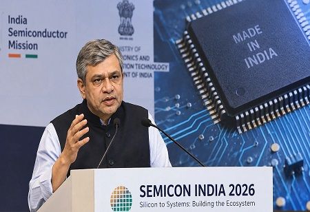
Minister of Union Electronics and IT Ashwini Vaishnaw reveals the target in Semicon India 2026, emphasizing the achievements that have been made during Semicon India 1.0. From the total number of 105 start-ups present in the first phase, about 20 get venture capital funding worth ₹800 crore. The next phase aims to extend this ecosystem further by promoting the creation of intellectual property, chip designs, and entire systems.
Also read: India, Myanmar Strengthen Maritime Ties with Naval Visit to Yangon
The Semicon India 2.0 initiative is more comprehensive in its attempts at developing semiconductor capacity within the country. This initiative focuses on six pillars, including chip design, semiconductor equipment & materials, foundry infrastructure, advanced packaging, R&D, and talent development. The approval by the Union Cabinet for this program comes with an investment plan of ₹1.275 lakh crore.
There is also more focus on equipment and materials. As per Vaishnaw, about $5 billion worth of investments in semiconductor machines and materials are being made at Semicon India 2026. The development of indigenous capability in such fields would help in decreasing supply chain dependencies and would offer an opportunity for Indian companies to get involved in the overall semiconductor industry ecosystem.
Talent development is yet another critical aspect of the programme. In phase one, the government aims at developing about 85,000 design engineers in the field of semiconductors in a period of ten years, with 70,000 getting trained within four years, says Vaishnaw. The plan under Semicon India 2.0 includes developing 1 lakh technicians, both clean room staff and on-the-factory-floor workers.
Also read: Indian mining sector's transformative journey towards a sustainable future
The other thing that the government is doing is focusing more on industrial research and closer collaboration between universities and firms. The India Semiconductor Mission 2.0 is meant to facilitate applied research along with developing expertise throughout the semiconductor ecosystem.
With the set of new objectives, India wants to create a holistic semiconductor ecosystem which will be based on semiconductor design, manufacturing, packaging, equipment, material, R&D, and manpower. The objective behind this mission is to develop the domestic capability and link Indian players in the global semiconductor value chain.